If you are into DIY guitar pedals and want to start designing your own effects, this article might help you open a few doors. I write this article as an EE student who earlier struggled with understanding these circuits and would often simply copy schematics off the internet.
This article is intended for-
1. Absolute beginners who like tinkering with electronics
2. Anyone who has been learning analog circuits and is looking for a jumpstart project.
Also before I start I'd like to mention, for anyone who wants to get a rock-solid foundation in Analog electronics, I highly recommend reading the book, 'Electronic Principles' by AP Malvino and David Bates.

The raw signal coming from the guitar is first amplified a little, and then the peaks of the amplified signal are clipped off by diodes (discussed ahead), thus changing the shape of the signal.
The extent to which the amplified signal is clipped off (discussed ahead) gives the effect its characteristic sound and name.

2.

3.
In the above plot, the blue curve is the final output ( VC (AC) ) after the DC component has been filtered out by the coupling capacitor (C6). And the green curve is the total collector voltage i.e VC (DC) + VC (AC).
This article is intended for-
1. Absolute beginners who like tinkering with electronics
2. Anyone who has been learning analog circuits and is looking for a jumpstart project.
Also before I start I'd like to mention, for anyone who wants to get a rock-solid foundation in Analog electronics, I highly recommend reading the book, 'Electronic Principles' by AP Malvino and David Bates.
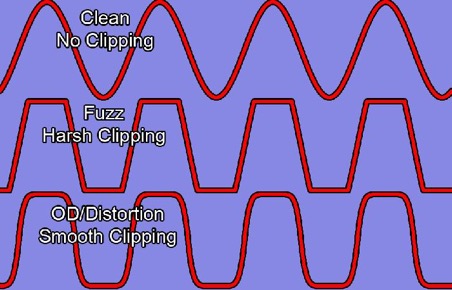
Distortion Pedals come in all flavors and sizes, however, how the distortion effect is achieved in any of the pedals is more or less similar. Let's first see how the output of the pedal compares to its input.
 |
| Image Credits- Wikipedia Commons |
The raw signal coming from the guitar is first amplified a little, and then the peaks of the amplified signal are clipped off by diodes (discussed ahead), thus changing the shape of the signal.
In a nutshell, every distortion pedal has a-
- Preamp Stage
- Clipping Stage
The extent to which the amplified signal is clipped off (discussed ahead) gives the effect its characteristic sound and name.

The best way to learn electronics is to analyze the master's work. If you Google- 'Distortion Pedal schematics', you'll see several circuits that are in some way similar to one- another. Let's pick up a random circuit and understand how it works.
1.
1.
3.
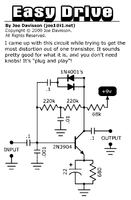
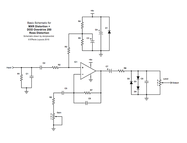
The first two circuits use a single transistor for amplification (and are very similar to one another) and the third circuit, uses an Opamp. And all of them use diodes for the clipping stage.
For the purpose of explanation, let's have a closer look at the second circuit titled- 'Easy Drive'.
To begin with here's the same schematic broken down into different sections, and we'll discuss section separately. (if you plan to read the whole article, I suggest, you open the image below in another tab, so that you can refer to it whenever required)
Such a capacitor is called a coupling capacitor. In a circuit like this one, that contains a DC voltage source and a DC component of current everywhere in the circuit, the coupling capacitor ensures that no DC current is fed back into the guitar's input.
A capacitor always acts as an open circuit for DC and as a short for AC. **
A simple clipper circuit's response to a 1V sine wave is shown below.
There's a pretty standard way of analyzing any transistor amplifier or transistor circuit in general. It involves analyzing the DC and AC currents flowing in it separately. The voltage at any point in the circuit is given by the sum of the DC and AC voltages at that point.
V=VDC + VAC
While the AC component makes the signal oscillate about the X-axis (for instance a sine wave), the DC component adds a bias to the center. The sine wave remains a sine wave just that its center is shifted up or down by a constant - VDC. This also implies that the DC gain(amplification factor) is different from the AC gain.
What follows next is an easy algorithmic approach to understand this section of the circuit.
At the is the point, you might want to ask yourself, what exactly are we trying to understand about the preamp stage?
One of the most logical things would be finding the AC amplification factor or in other words, finding out 'how much' does the amplifier amplify a given signal.
STEP 1 - DC Analysis
Obtain the DC equivalent circuit by removing all capacitors i.e open circuiting them. Our aim from this step would be to calculate the emitter current (current through R4) as we would need it later.
What we've obtained from the DC equivalent circuit is a very popular type of transistor biasing called 'Collector- and emitter-feedback bias'.
Putting in the component values from our circuit we get,
For the purpose of explanation, let's have a closer look at the second circuit titled- 'Easy Drive'.
To begin with here's the same schematic broken down into different sections, and we'll discuss section separately. (if you plan to read the whole article, I suggest, you open the image below in another tab, so that you can refer to it whenever required)
1. The Input Stage-
The input stage is simply the guitar's input coupled to a capacitor (C1).Such a capacitor is called a coupling capacitor. In a circuit like this one, that contains a DC voltage source and a DC component of current everywhere in the circuit, the coupling capacitor ensures that no DC current is fed back into the guitar's input.
A capacitor always acts as an open circuit for DC and as a short for AC. **
2. The Output Stage-
The output stage consists of the output jack with a coupling capacitor (C6), as what goes to the amplifier, must not contain any DC component (unless you've decided to test your amp to the extreme conditions and your neighbor's temper as well).3. The Clipping Stage-
The amplified signal is clipped by two diodes- D1 and D2. To understand why clipping occurs you need to understand how a diode responds to the voltage across it. And this video does a great job of explaining the same. The key idea remains that diodes must be connected parallelly with the output to observe clipping.A simple clipper circuit's response to a 1V sine wave is shown below.
4. The Preamp Stage-
Finally, the preamp in this circuit uses a single NPN transistor. The transistor is a versatile component and has a steep learning curve associated with it. I highly recommend either reading the book mentioned above or watch this video to get a quick idea. The purpose of this section is not to explain everything under the sun but to develop a brief idea and intuition for analyzing such circuits.There's a pretty standard way of analyzing any transistor amplifier or transistor circuit in general. It involves analyzing the DC and AC currents flowing in it separately. The voltage at any point in the circuit is given by the sum of the DC and AC voltages at that point.
V=VDC + VAC
While the AC component makes the signal oscillate about the X-axis (for instance a sine wave), the DC component adds a bias to the center. The sine wave remains a sine wave just that its center is shifted up or down by a constant - VDC. This also implies that the DC gain(amplification factor) is different from the AC gain.
What follows next is an easy algorithmic approach to understand this section of the circuit.
At the is the point, you might want to ask yourself, what exactly are we trying to understand about the preamp stage?
One of the most logical things would be finding the AC amplification factor or in other words, finding out 'how much' does the amplifier amplify a given signal.
STEP 1 - DC Analysis
Obtain the DC equivalent circuit by removing all capacitors i.e open circuiting them. Our aim from this step would be to calculate the emitter current (current through R4) as we would need it later.
What we've obtained from the DC equivalent circuit is a very popular type of transistor biasing called 'Collector- and emitter-feedback bias'.
In such a biasing configuration, by applying Kirchoff's Voltage Law, the emitter current (through RE) is given by-
β = 200 (The DC current gain of the transistor as mentioned in its datasheet)
VBE= 0.7 (Forward voltage drop of the base-emitter diode, inside the transistor)
Vcc= 9V
RE = 680Ω
RB=440kΩ
Rc= 68kΩ
Putting in the component values from our circuit we get,
IE=0.12mA (We'll need this value in the next step)
Being equipped with this data, we can also find out the DC component of the preamp's output (although the output coupling capacitor filters out the DC component of current). You can skip to STEP 2 without loss of continuity.
According to the transistor current equation,
IE=IB+IC
And since is IB very small, we can approximate (typical engineer move)
IC ≈ IE =0.12mA
VC = Voltage at the collector terminal w.r.t GND
VC= Vcc - ICRC
And so VC (dc)= 0.84V
This means the DC component of the collector voltage is 0.84 V, or in other words whatever AC voltage appears at the collector will be shifted up by 0.84V.
 |
| A simulation of the same circuit on LTspice |
And if you measure the vertical distance between any two crests or peaks you will find that it is almost 0.84V!
re’ (part of the Ebers Moll equivalent) is ac resistance of the base-emitter diode. It can be easily calculated by using the formula-
re’= 25mV / IE
In our case, re’= 25mV/0.12mA = 208Ω
To get the value of the resistor, we multiply this value by β-
βre’=42kΩ
Finally, all you need to do is re-draw the circuit, in a way that the input and output circuits can be understood separately. Before you proceed, convince yourself that the circuit below is the same as the previous circuit, just that it's better organized.
Finally, to calculate the AC amplification factor we, just need to compare the output of the circuit (tagged output), to the input guitar signal. The AC voltage source in all the diagrams is the guitar signal.
AC Voltage Gain ( amplification factor ) = vout/vin
vin = ib * 42k
For vout, we need to find the voltage across the equivalent resistance for R3 and R5 connected in parallel.
vout = βib * 52k
vout/vin= 1.23 * β
with β= 200,
we have -
AC Voltage Gain ( amplification factor ) = vout/vin = 247
This means if you feed the amplifier with a 10mV (peak-to-peak) signal you obtain an amplified version of that signal at the output that's almost 2.47 V (peak-to-peak).
Having said that, we have 'analyzed' the preamp's amplification!
Now, if you clip the output voltage using two diodes connected to GND, the peak voltage would be limited to nearly -0.7v to 0.7 V (for typical diodes) with the signal getting squarish and distorted. This is what happens in the very first circuit of the three examples we saw above (scroll up!). However, in this circuit, we don't directly clip the output signal instead clipping happens through a feedback path that connects the output back to the input of the amplifier stage but through two diodes!
Before we end our discussion, I want to talk about all the assumptions we've made to simplify the process and understand it better, that may be a bit far from reality.
1. The capacitors don't act as perfect short circuits for AC signals.
The impedance of a capacitor is a function of its capacitance and frequency of the signal across it.
If the product of its capacitance and frequency of the signal is a number big enough to make its impedance negligible, we directly replace the capacitor with a short.
This is why we open-circuited C4, instead of shorting it. C4 is a filtering capacitor; whenever there's high-frequency noise/squeak in coming in from the guitar's input, its impedance decreases and allows the noise to be directed to the ground, hence preventing the noise from being amplified. This called also called passive low pass filter.
2. The value of β varies from transistor to transistor and is not constant even for a given transistor.
There are a lot of factors on which the value of β depends on. But for most calculations, we can approximate its value to a number provided in that datasheet.
Even such subtle squarish-ness can create significant audible distortion in the sound.
That's all for this article. I hope this article has equipped you with a better understanding of distortion circuits. If you enjoyed reading this article and would like to see more similar articles, do let me know by leaving a comment below!
Cheers,
Siddharth
That's definitely quite an overkill for a 'STEP 1'.
STEP 2- AC Analysis
Since the input signal from the guitar is a pure AC signal and so is the final output (as it goes through a coupling capacitor), this is the most important step in the entire procedure. At this point it's worth mentioning, as a convention, all AC voltages and currents are represented by lowercase letters. There are quite a few elements that make up this step-
- Short all capacitors and DC voltage sources, except for C4 which should be open-circuited for reasons that I'll discuss later in the article. Also, for now, let's deal with the preamp stage isolated from the clipping stage.
- Replace the transistor with an equivalent Ebers-Moll Model. The transistor as a whole can be broken down into simpler components called an equivalent model. One such transistor equivalent model is the- Ebers Moll model.
The Ebers Moll Model
re’ (part of the Ebers Moll equivalent) is ac resistance of the base-emitter diode. It can be easily calculated by using the formula-
re’= 25mV / IE
In our case, re’= 25mV/0.12mA = 208Ω
To get the value of the resistor, we multiply this value by β-
βre’=42kΩ
Finally, all you need to do is re-draw the circuit, in a way that the input and output circuits can be understood separately. Before you proceed, convince yourself that the circuit below is the same as the previous circuit, just that it's better organized.
Finally, to calculate the AC amplification factor we, just need to compare the output of the circuit (tagged output), to the input guitar signal. The AC voltage source in all the diagrams is the guitar signal.
AC Voltage Gain ( amplification factor ) = vout/vin
vin = ib * 42k
For vout, we need to find the voltage across the equivalent resistance for R3 and R5 connected in parallel.
vout = βib * 52k
with β= 200,
we have -
AC Voltage Gain ( amplification factor ) = vout/vin = 247
This means if you feed the amplifier with a 10mV (peak-to-peak) signal you obtain an amplified version of that signal at the output that's almost 2.47 V (peak-to-peak).
Having said that, we have 'analyzed' the preamp's amplification!
Now, if you clip the output voltage using two diodes connected to GND, the peak voltage would be limited to nearly -0.7v to 0.7 V (for typical diodes) with the signal getting squarish and distorted. This is what happens in the very first circuit of the three examples we saw above (scroll up!). However, in this circuit, we don't directly clip the output signal instead clipping happens through a feedback path that connects the output back to the input of the amplifier stage but through two diodes!
Before we end our discussion, I want to talk about all the assumptions we've made to simplify the process and understand it better, that may be a bit far from reality.
1. The capacitors don't act as perfect short circuits for AC signals.
The impedance of a capacitor is a function of its capacitance and frequency of the signal across it.
If the product of its capacitance and frequency of the signal is a number big enough to make its impedance negligible, we directly replace the capacitor with a short.
This is why we open-circuited C4, instead of shorting it. C4 is a filtering capacitor; whenever there's high-frequency noise/squeak in coming in from the guitar's input, its impedance decreases and allows the noise to be directed to the ground, hence preventing the noise from being amplified. This called also called passive low pass filter.
2. The value of β varies from transistor to transistor and is not constant even for a given transistor.
There are a lot of factors on which the value of β depends on. But for most calculations, we can approximate its value to a number provided in that datasheet.
Putting it all together-
Here's how the final output of the entire circuit compares to the original signal.
Here's a slightly zoomed-in view to observe how the output's peak has become a little squarish.
Even such subtle squarish-ness can create significant audible distortion in the sound.
That's all for this article. I hope this article has equipped you with a better understanding of distortion circuits. If you enjoyed reading this article and would like to see more similar articles, do let me know by leaving a comment below!
Cheers,
Siddharth


Comments
Post a Comment